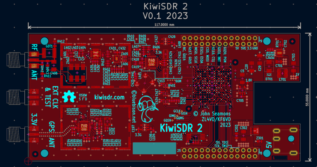
KiwiSDR 2 Goals:
Minimal changes. Fastest time-to-market with lowest possible risk. BUT since the PCB is going to be re-spun fix some of the known limitations that don’t add too much risk:
- New RF front-end:
- Balanced input via balun transformer
- Digital attenuator (per the advisory group: pSemi PE4312, 0 – 31.5 dB, 0.5 dB steps)
- Gas discharge tube (GDT) across input in addition to TVS diodes
- Static drain resistors (100K) from input connections to ground
- External ADC clock brought out on third SMA connector
- Self test loopback mode using a short cable between this SMA and antenna input
- New GPS chip to replace current one which is now EOL
- Reverse polarity protection (via P-FET) on 5V DC input
- TVS diode across 5V input
Source: http://www.kiwisdr.com/
VISIT: http://www.kiwisdr.com/


